PCB Via Filling Explained
Par un écrivain mystérieux
Description
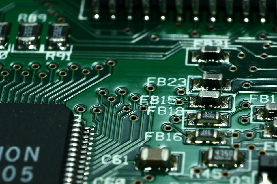
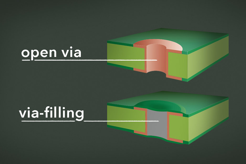
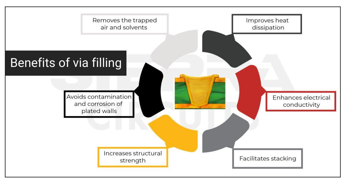
PCB Via Filling/Plugging is a process where the Via hole is filled with solder mask or resin to improve the reliability of the printed circuit board.

Plugging the Connection Gap: The Importance of Filled Vias in

PCB Via: An Ultimate Guide - NextPCB
Via Fill – Amitron U.S. PCB Manufacturer
Via hole protection, Via plugging
PCB: choose the type of VIA FILLING according to your needs - ALBA
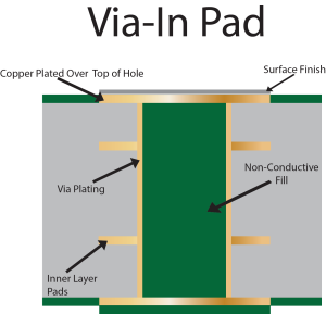
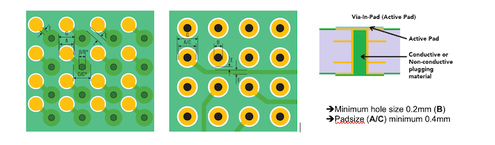
What are Vias in Pad? Advantages, Limitations, Applications, and

Schematic illustration of via filling process with molten solder

What is Via Filling? - PCB Directory
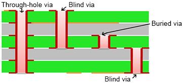
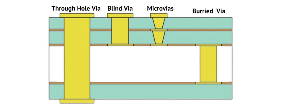
Blind Via PCB and Buried Via PCB
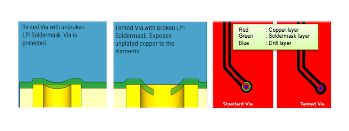
Via hole protection, Via plugging
Via Filling Techniques Designers Need to Know
depuis
par adulte (le prix varie selon la taille du groupe)


.jpg)